|
Product Name |
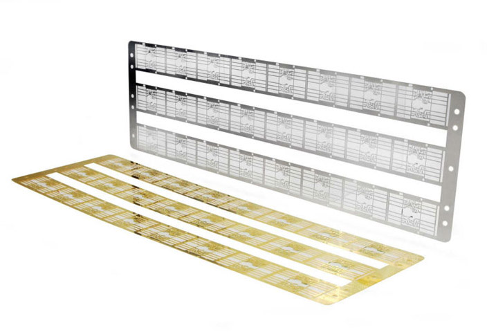
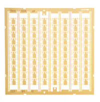
High-precision IC Lead Frames Components Etching |
|
Use |
various types of integrated circuit metal components |
|
Model |
Various models |
|
Product flatness |
0.2 or less (flatness our product can do 0.02) |
|
Minimum aperture |
0.08MM (0.03MM thick material can do 0.05MM) |
|
The minimum diameter |
0.025MM +/- 0.01MM |
|
Thickness |
0.03MM-1.0MM error is +/- 0.01 |
|
Proofing deadline |
48 hours |
|
Production and delivery |
on time or ahead |
|
Precision products |
+/- 0.01MM |
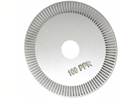
TVs, cell phones, communication devices, lock system, sports devices, cars, outdoor devices, household appliances, etc. Phone antenna is an essential component of the lead frame to receive signals for communications products. SinoGuide production of high precision, is the best choice instead of the Chinese production. Smooth and uniform burrs, flatness ismaintained at less than 0.02 is one of the characteristics of the antenna of the phone. Chemical etching works with many metals, including a wide variety alloys of iron, nickel, copper, aluminum; as well as molybdenum and silver.
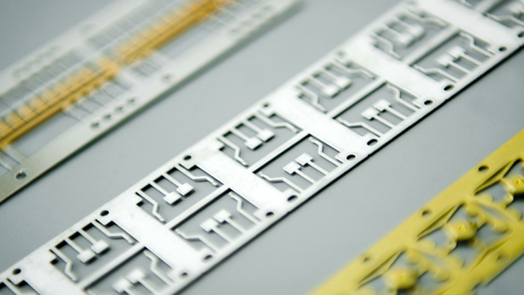
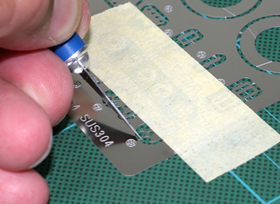
Continuous development of semiconductor process and design technologies has led to growing demand of thinner, smaller, and more complicated devices and packaging solutions. Etched lead frames become obvious choices than stamped ones given their superior precision features, ultra fine tolerances and much shorter delivery time.
Semiconductor Leadframes Etching
What is a Semiconductor leadframe? A Semiconductor leadframe is a thin layer of metal that connects the wiring from tiny electrical terminals on the semiconductor surface to the large-scale circuitry on electrical devices and circuit boards. Leadframes are used in almost all semiconductor packages.
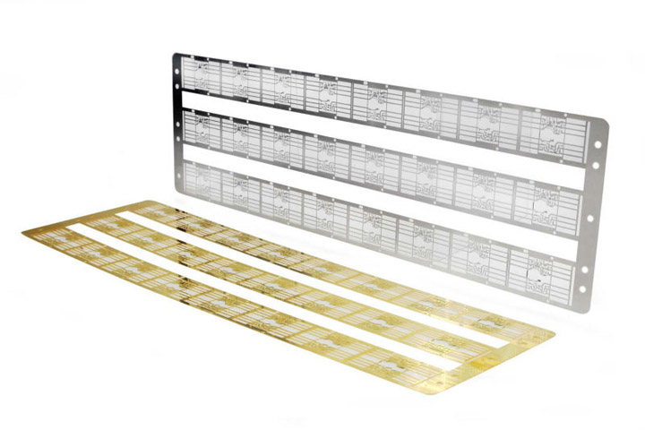
Leadframes manufactured by SinoGuide Etching are used in many industry sectors including semiconductors, relays, glass-to-metal seals and medical applications such as implantable devices and hearing aids. The significant advantage of SinoGuide photo etched leadframes is the ability to produce large quantities of product with less tooling `Wear’ so the last lead frame is exactly the same as the first leadframe. Changes to the photo tooling can be very quickly implemented and the modification to these tools is significantly less expensive than traditional hard tooling. The process is ideal for manufacturing from prototype through to production quantities.
Its applications include signals, lighting products/components with either visible or invisible light, and all kinds of optical products. In this field, we have possessed many core technologies and can provide total solutions for our customers. We design and manufacture photo etched components from various metals suitable for aerospace, defense, medical, electronic, filtration, automotive and many other commercial markets. Our core competency lies in producing micro-machined components, such as micro fluidic devices, screens and meshes, fuel valves, manifolds, electronic components and disc filters.
Please feel free to contact SinoGuide or any of our Sales Engineer to discuss your specific application requirement.


 +86-755-89375091